Dual PWM Step-Down Converter in a 2mm x
2mm Package for WCDMA PA and RF Power
14 ______________________________________________________________________________________
Input Capacitor Selection
The input capacitor (C
IN
) reduces the current peaks
drawn from the battery or input power source and
reduces switching noise in the MAX8896. The imped-
ance of C
IN
at the switching frequency should be kept
very low. Ceramic capacitors with X5R or X7R tempera-
ture characteristics are highly recommended due to
their small size, low ESR, and small temperature coeffi-
cients. A 4.7礔 capacitor is recommended for C
IN1
and
2.2礔 for C
IN2
. For optimum noise immunity and low
input ripple, the input capacitor value can be
increased.
Note that some ceramic dielectrics exhibit large capac-
itance and ESR variation with temperature and DC bias.
Ceramic capacitors with Z5U or Y5V temperature char-
acteristics should be avoided.
Thermal Considerations
In most applications, the MAX8896 does not dissipate
much heat due to its high efficiency. But in applications
where the MAX8896 runs at high ambient temperature
with heavy loads, the heat dissipated may exceed the
maximum junction temperature of the part. If the junction
temperature reaches approximately +160癈, the thermal-
overload protection is activated.
2MHz
OUT1
LX1
PGND1
PAOUT
IN1
RFEN1
REFIN
REF
REFBP
*DE2818C
AGND
LDO
IN2
PAEN
CONTROL
PA ENABLE
RF ENABLE 1
ANALOG
CONTROL
2MHz
OUT2
LX2
PGND2
RFEN2
OUT2
1000pF
RF ENABLE 2
2.7V TO 5.5V
0.1礔
V
CC
4.7礔
0.033礔
2.2礖
BRL2012T 2R2M
2.2礔
V
RF
(2.8V)
2.2礔
4.7礖*
V
PA
4.7礔
MAX8896
V
OUT2
(3.1V)
LDO
OUT2
1礔
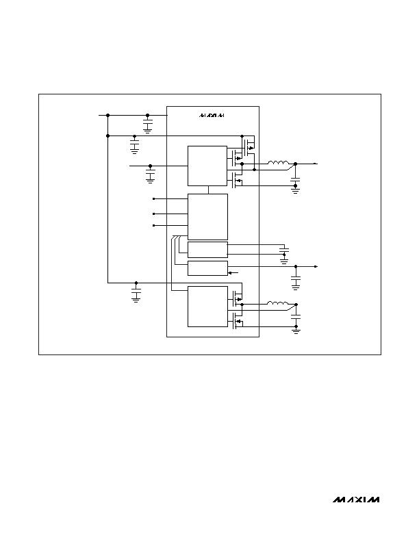
Figure 3. Typical Applications Circuit
发布紧急采购,3分钟左右您将得到回复。
相关PDF资料
MC33232PG
IC PFC CONTROLLER CRM 8DIP
MC33260DR2G
IC PFC CONTROLLER DCM 8SOIC
MC33262DG
IC PFC CONTROLLER CRM 8SOIC
MC33368DR2G
IC PFC CONTROLLER CRM 16SOIC
MC33567D-1G
IC REG CTRLR DUAL OUT 8-SOIC
MCP18480T-I/SS
IC HOT SWAP CTRLR -48V 20SSOP
MCP9808T-E/MS
IC TEMP SENSOR DGTL I2C 8MSOP
MCZ33998EGR2
IC REG CHARGEPUMP/LINEAR 24SOIC
相关代理商/技术参数
MAX8896EREE-T
制造商:Maxim Integrated Products 功能描述:
MAX8896EVKIT+
功能描述:直流/直流开关转换器 Dual PWM Step-Down Converter in a 2mm x 2mm Package for WCDMA PA and RF Power RoHS:否 制造商:STMicroelectronics 最大输入电压:4.5 V 开关频率:1.5 MHz 输出电压:4.6 V 输出电流:250 mA 输出端数量:2 最大工作温度:+ 85 C 安装风格:SMD/SMT
MAX8899EVKIT+
制造商:Maxim Integrated Products 功能描述:EVALUATION KIT FOR MAX8899 - Boxed Product (Development Kits)
MAX8899EWZ+
制造商:Maxim Integrated Products 功能描述:- Rail/Tube
MAX8899EWZ+T
制造商:Maxim Integrated Products 功能描述:WCDMA/EDGE/GPRS/GSM/CDMA - Tape and Reel
MAX8899EWZ+TCAA
制造商:Maxim Integrated Products 功能描述:WCDMA/EDGE/GPRS/GSM/CDMA PHONE PMIC - Rail/Tube
MAX8899GEWZ+
制造商:Maxim Integrated Products 功能描述:- Rail/Tube
MAX8899GEWZ+T
制造商:Maxim Integrated Products 功能描述:PMIC FOR MSM 7XXX SERIES ANALOG BASE BAND - Tape and Reel